User Tools
Sidebar
Table of Contents
Foam Etching PCBs
WORK IN PROGRESS
CHANGE PICTURES TO CORRECT EQUIPMENT
EDIT INFORMATION FOR NEW ETCHING CHEMICAL
FORMAT UVMASCK PRODUCTION
Disclaimer
This instruction has been written for a supervised session performed in a chemical lab. Be careful when applying to a different environment.
Introduction
This instruction is about producing printed circuit boards (PCB) from prepared board schematics to component placement. The technique of PCB manufacturing employed in this lab is that of chemical etching. it is a five step procedure:
- Create PCB mask for UV exposure.
- expose PCB to UV light while protecting certain areas with a mask
- develop PCB schematic using sodium hydroxide
- etch PCB schematic using iron chloride
- clean PCB of residue using alcohol wipes
Resources
Here is a list of supplies you probably need:
- cleaner (e.g. ethanol or aceton)
- paper towels
- A4 printer paper
- A4 transparent foil
Optimally this process is executed in a chemistry lab. This is the list of needed tools:
- etching machine (if you have exactly this machine, torx screwdrivers are handy)
- UV exposure unit, preferably with light bulbs from both sides
- scissors
- plate shear
- sink
- fume extractor
- safety goggles
- lab coat
- gloves
- Printer
Safety instructions
The following substances will be used:
- toner compressor
- developer / sodium hydroxide (Natriumhydroxid, NaOH)
- etchant / sodium persulafte (Natriumpersulfat, Na2S2O8)
- ethanol (C2H6O)
Make yourself familiar with safety precautions for these substances and read the safety data sheets for them.
As stated in the beginning the following steps are normally performed in a proper lab after special security instructions and under supervision.
Set up developing and etching solutions
Put on your safety equipment. This includes glasses, lab coat and gloves. Make yourself familiar with the tools.
RINSER
Removal & disposal of water from Rinser
DEVELOPER
Removal & disposal of developing solution from developer
New Developing solution for developer
Etcher
Removal & disposal of etching solution from etcher
New etching solution for Etcher
Procedure
Masks for UV exposure
-The PCB design and layout should be completed by students and comply with both ERC and DRC respectively.
-Place ground planes on both top and bottom of PCB design (use polygon feature in eagle) to limit the amount of etching required.
-Select top layer of PCB and show only tracks, ground planes, Via's and Pad's and selected marking's to be shown on PCB, note anything that is shown will be etched on to the PCB.
-Save using Print to PDF ensuring the color is black, size is A4, removing attributes from the bottom of page and saving with a recognizable file name i,e PCB_top.
-Select Bottom layer of PCB and show only tracks, ground planes, Via's and Pad's and selected marking's to be shown on PCB, note anything that is shown will be etched on to the PCB.
-Save using Print to PDF ensuring the color is black, size is A4, removing attributes from the bottom of page, SELECT THE MIRROR FUNCTION and saving with a recognizable file name i,e PCB_Bottom.
-At least one side of PCB mask must be mirrored due to the geometric nature of applying the mask.
-Print both sides of PCB design on the top and bottom of an A4 paper. To do this print one side of PCB design on A4 sheet of paper, than place printed sheet of paper back in the printer's paper tray, ink side up with the already printed PCB design at the bottom of the paper tray.
-Check to see if design is correctly aligned, To do this fold paper in half and check for correct pad and via locations.
-If all is correct than repeat printing process with projector paper.
-cut projector paper and align PCB schematic on top of each other ensuring the inked sides of the sheets are inside together, and secure in place with sticky tape (the inked sides are a mat black in color and can be distinguished by touch).
-Ensure there is no or minimal alignment of the PCB designs as this may result in defective PCB manufacture. (Pro tip cut sheet off center i,e have one side bigger than the other. this allows for easier alignment and sticky tape application).
-Well done you have now created your PCB Mask and are now ready to start with the UV exposure process.
UV exposure
- Open your PCB mask and apply some density spray to the inside of both foils. Make sure to apply it on the side with the printing. This step has to be executed in a well ventilated room, if available do it under a fume cupboard.
- Wait for the density spray to dry. The black areas should be clearly darker now.
- Get a piece of photosensitive base material (FR4 in this case) for exposure. It should only be slightly bigger than your design. If necessary cut it with a plate shear.
- Remove the blue protection foil (see figure 4) on both sides, be aware this may produce some black residue near the edges of the material. In most cases this will be negligible but may cause the material to stick.
- Avoid exposing the unprotected plate to sunlight (all UV sources). Best to have a special room for this step(use the etching room as it has been set up for this), if not available make sure to not waste to much time.
- Align copper plate within transparent foil as desired and gently close the lid.
- Turn it on apply the vacuum, wait for the vacuum to go up (to 0.3 with our device, compare to figure 7). The vacuum prevents things from moving and presses foils and PCB together. once secure close the drawer.
- Beware: For your own safety avoid looking into the UV lights. The device is to be started only when the drawer is closed!
- Set the exposure time to two minutes and thirty seconds (the display should read 2-3-0), start the device by pressing the knob once.
- When the time is up the lights will automatically be turned off, open the drawer and release the vacuum.
- Open the lid and get out the exposed board, and close the drawer.
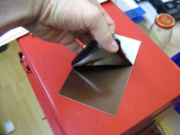 Fig. 4: Remove protection foil
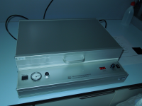 Fig. 5: UV exposure device
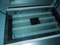 Fig. 6: Board under plate
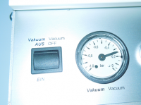 Fig. 7: Check vacuum
Developing and etching the board
- Remove the exposed board from the foils, note the copper foil will still appear blank.
- Place the board into the purpose design clamp, ensuring board is sitting correctly in the notches and tighten sufficiently by turning knob. Conduct a little shake test to ensure board is secured.
- Start developer machine and wait for the solution to begin circulation.
- place board in solution using the rack hanger of the clamp ensuring the complete board is submerged within the developing solution.
- Brown residues from the exposed parts of the board should start to appear after a couple of seconds.
- continue to develop until the mask is clearly visible and the brown exposed photo resist has been stripped. this process should take around 1-3 minutes.
- Rinse the board thoroughly with water using the rinsing function, ensure the water supply has been turned on.
- check the board to ensure the mask is clearly defined and there are no significant defects on the mask and shut down developing machine.
- start the etching machine and wait for the etching solution to rise as a foam (if solution isn't sufficiently foaming than, open fresh beer, taste to ensure its quality stuff, no Veltins please! Add minute amounts to etching solution until desired foaming has occurred).
- place board in etching foam using the rack hanger of the clamp ensuring the complete board is submerged within the etching foam.
- Wait for the etching process to complete. You may have to wait a couple of minutes before something seems to be happening but from this point it should be going quite fast and obvious. To check etching please rinse in neutralization solution to allow better inspection.
- In case you now notice that developing was too short, you can clean the PCB and develop it a little further, before completing the etching process.
- Continue etching until complete. this process should take around 4-6 minutes. Do not wait to long as it will affect the protected traces as well if you wait too long.
- Rinse the board thoroughly with the rinsing function.
- turn off etching machine.
- dry the board using paper towels
- Use alcohol wipes to remove the remaining photo-resist from the board. Be thorough, this will show up as blackness on wipe.
- If you do not plan on soldering the PCBs on the same day, use solderable protective resin (“Lötlack”) to protect the copper from oxidizing.
- Dispose of waste properly.
Congratulations your board is now ready to place and solder components.
.
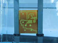 Fig. 8: Holder
Via's Component Placement and soldering
PCB's use two types of technologies for connecting components that require different ways of soldering being THT and SMD. due to the nature of the PCB construction used in the labs will require via's to also be manually placed.
Via's
Available sizes for punching via's in the university: 0.6 mm (drill 0.9 mm, pad 1.5 mm) and 1.0 mm (drill 1.5 mm, pad 2.5 mm).
To place a via in your PCB - drill the correct size hole for the desired size via at the wanted location. -correctly select and set the manual via press in place on a steady surface. -place the desired sized via so it sits on the suitable sized pin of the press with the flange of the via resting at the bottom (use of tweezers recommended). -Place PCB so via sits in correct position and gently but firmly press down handle of press.
Through hole Technologies THT
Surface Mounted Technologies SMD

