Sidebar
EAGLE Tutorial
We will use EAGLE to design a printed circuit board (PCB) in this lab. We will use a free version in the lab but Autodesk provides its professional version free of charge to students after registration:
https://www.autodesk.com/products/eagle/free-download https://www.autodesk.com/support/technical/article/caas/sfdcarticles/sfdcarticles/Eagle-Education.html
EAGLE works in two steps, first, you have to create a schematic of your circuit. This is pretty straightforward as it uses standard primary symbols in its editor. The second step is positioning the components on a PCB and laying out (routing) the connections (traces) between them.
The task is to design a PCB for
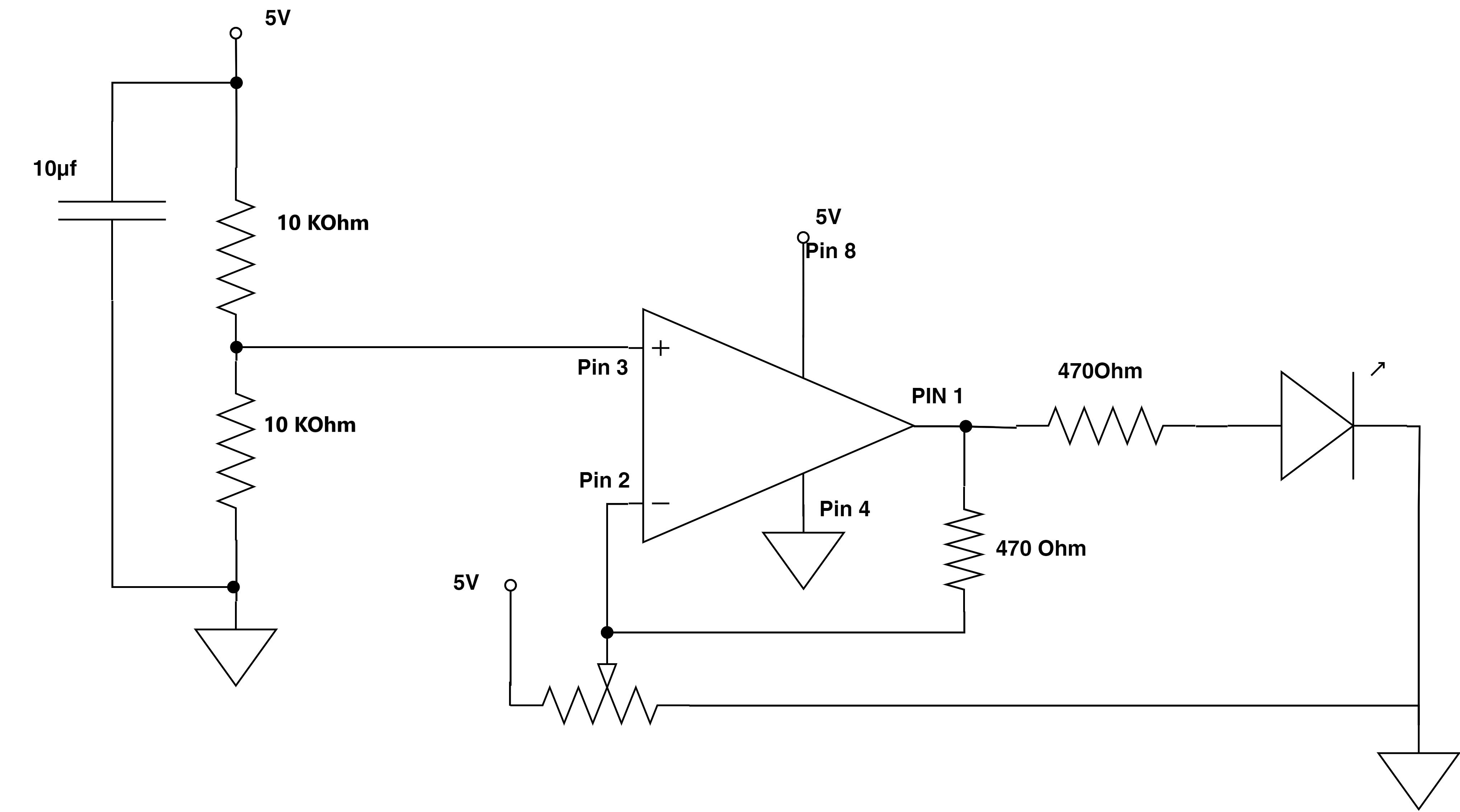
Voltage Divider Circuit with LM358 Op-Amp, Potentiometer, and LED Output
Description:
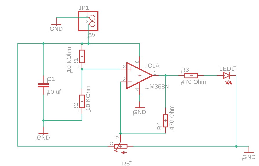
This circuit is designed to create a voltage divider using an LM358 operational amplifier (op-amp) with the output connected to an LED for visual output indication. The voltage to be divided is applied to the non-inverting input of the op-amp through a voltage divider, while a potentiometer is connected to the inverting input, allowing for voltage control.
Components
Remember the difference between through-hole technology (THT) and surface-mount device (SMD) components to choose the appropriate one based on the type of component you have
list of Components
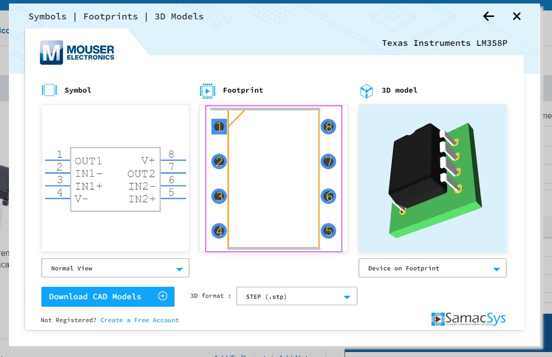
• LM358, Operational amplifier, Through hole, Two Op-Amps in one device
• Resistor, 10KOhm - 470 Ohm, SMD Package 1206, 4 pcs
• Capacitor, 10µF, SMD Package 1206, 1 pcs
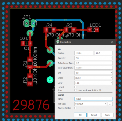
• Pin Header, 1×2, THT, pitch 2.54mm
• potentiometer, THT, 10kOhm
• LED, SMD 1206, Green
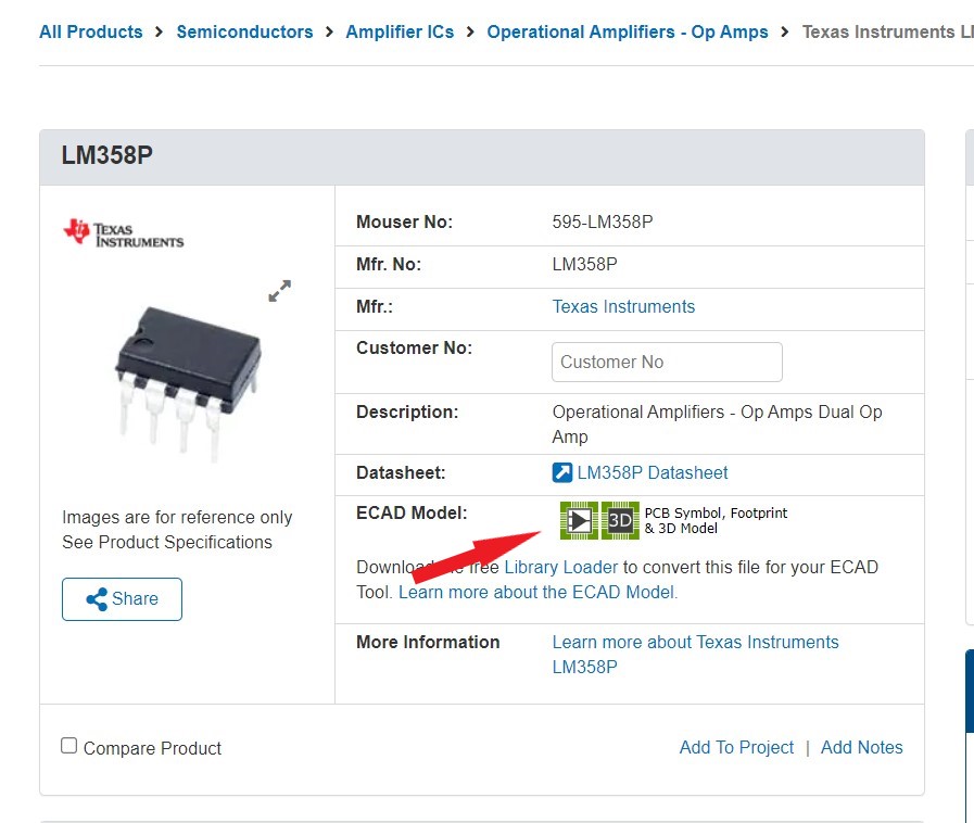
Every component has an ECAD model which includes a Circuit symbol for the schematic, a Footprint for the board layout, and a 3D Model
Schematic
The following steps will guide you through the creation of the schematic file…
1. Start the EAGLE software from your computer's start menu.
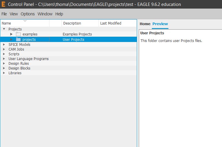
2. In the EAGLE menu, locate the 'Projects' section and expand it.
3. Right-click on the 'project' folder and choose 'New Project.' Give your project a name.
4. Right-click on the project folder you created and select 'New' and then 'Schematic.'
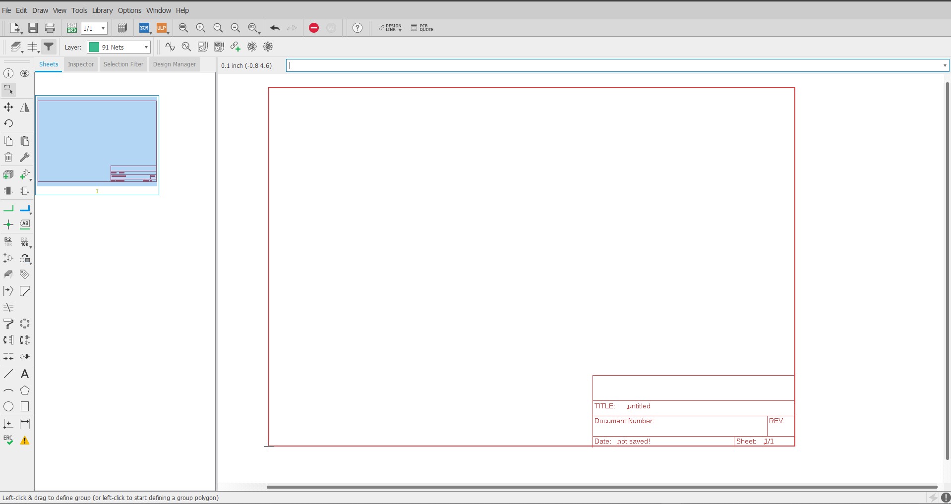
5. In the new schematic window, go to 'File' and choose 'Save' to save your schematic file.
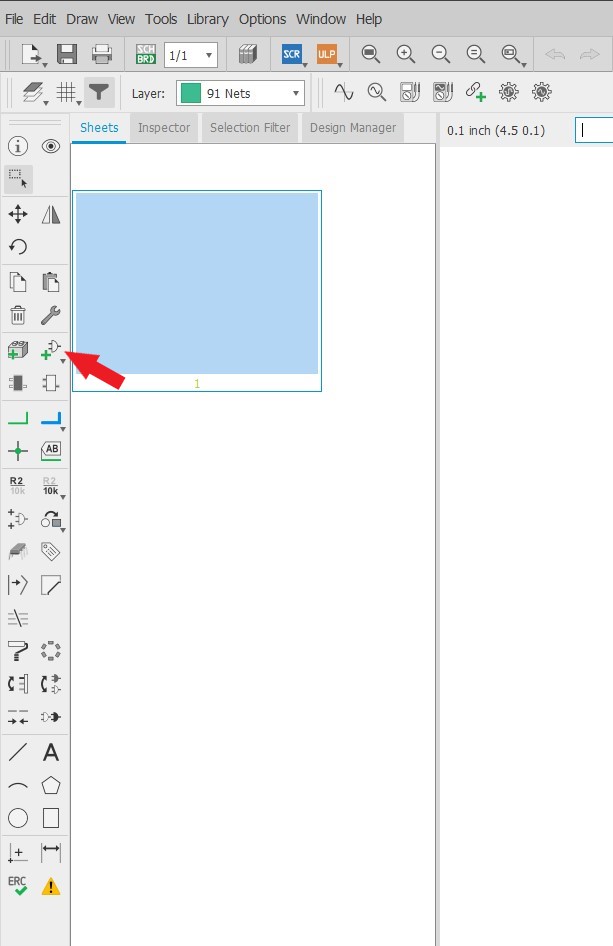
6. Begin your work by adding a frame to the document sheet. Click on the 'Add' icon on the left side of the EAGLE interface. In the new window, expand the 'frames' library and select “DINA4_L.” Click 'OK.' Click anywhere in the blank area to add the frame to your schematic. This frame will contain all the schematic components.
7. Press the 'ESC' key twice. Use the mouse wheel to zoom in or out until you can see the entire frame. Hold the mouse wheel to move around the schematic.
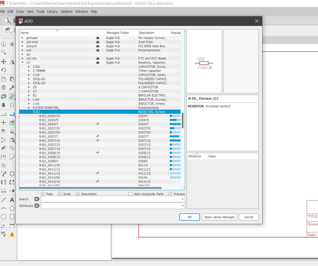
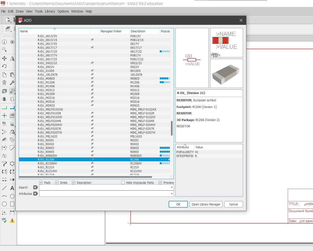
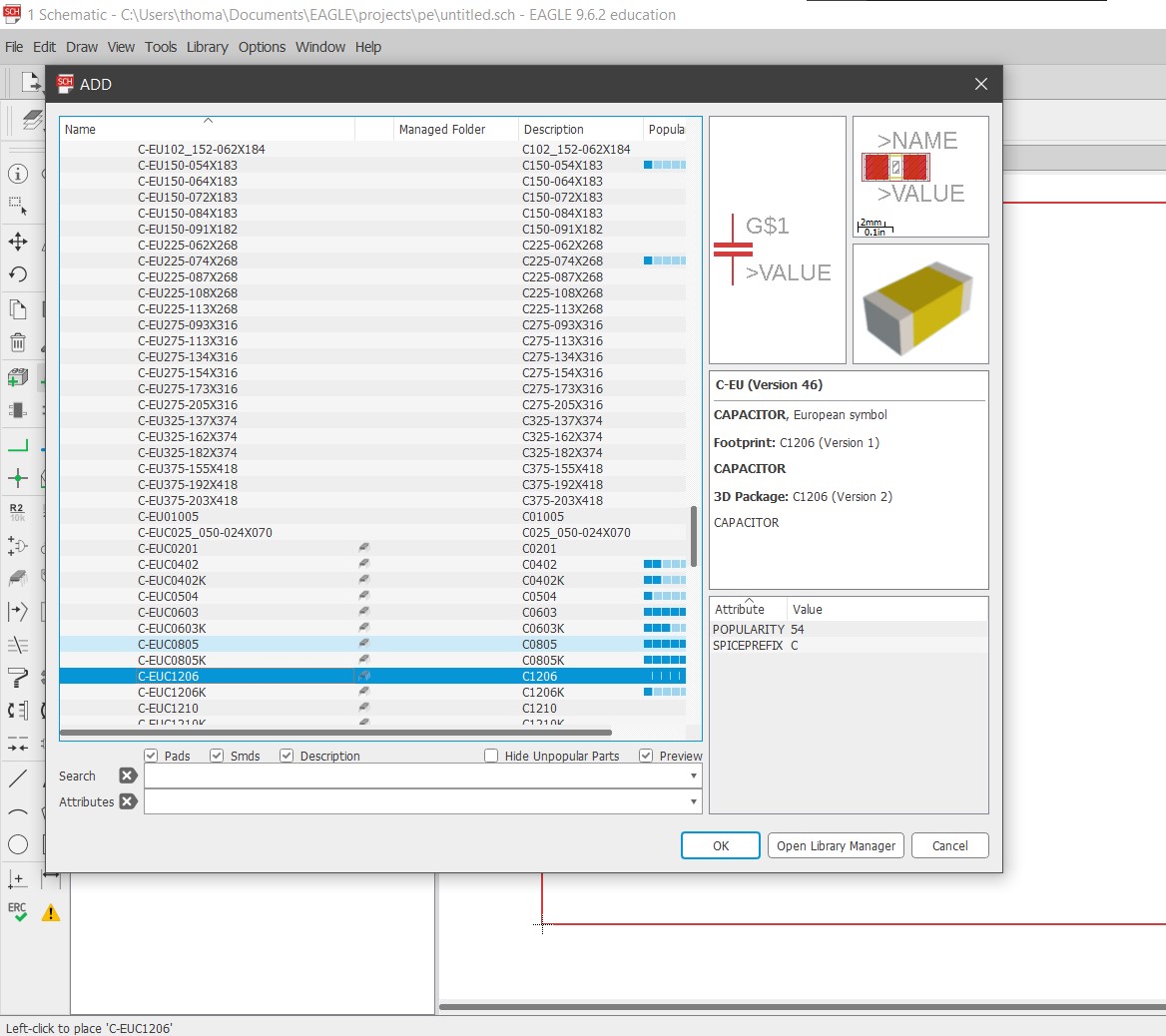
8. Start by adding resistors and capacitors. Click on the 'Add' icon again. Go to the 'rcl' library and select 'R-EU' then choose 'R-EU_R1206' for resistors. Place four of them. You can right-click before placing a component to rotate it. Similarly, add a capacitor from the 'C-EU' then choose 'CEUC1206'.
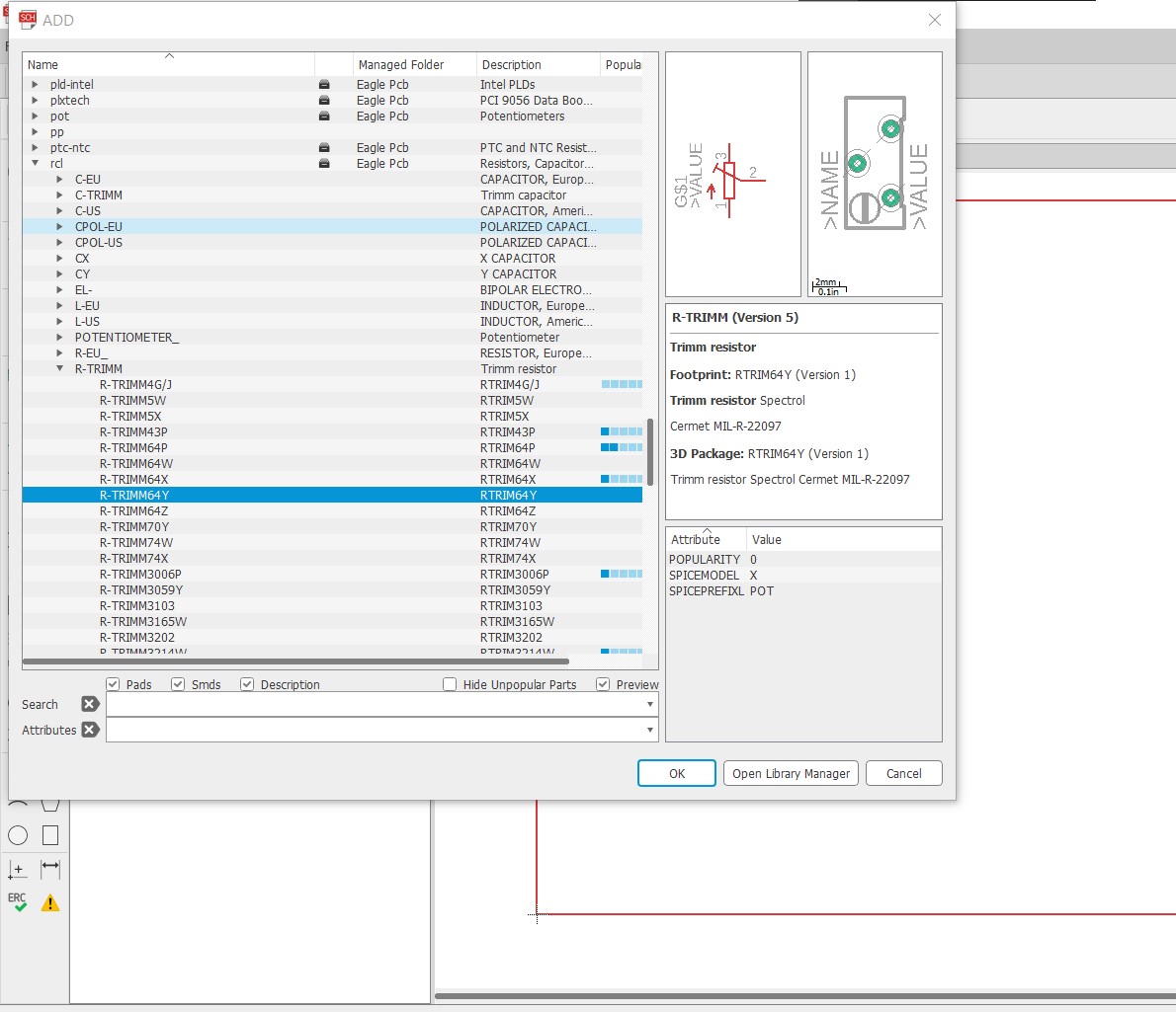
9. In the 'rcl' library, locate the potentiometer 'R-TRIMM64Y' and add it to your schematic.
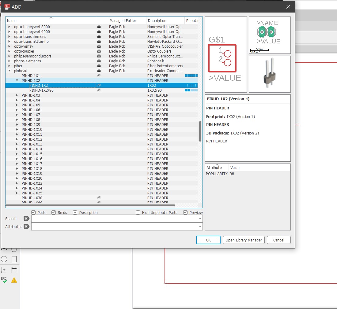
10. Additionally, add a connector from the 'pinhead' library, 'PINHD1X2.' for the supply.
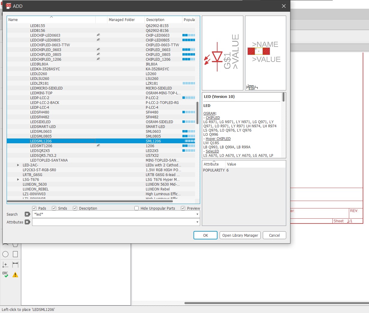
11. In the 'LED' library, look for 'LEDSMT1206'and add one to your schematic.
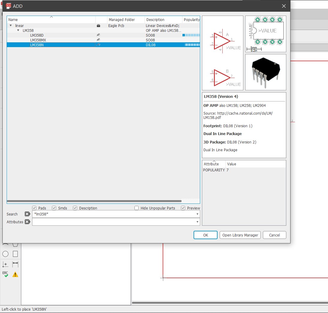
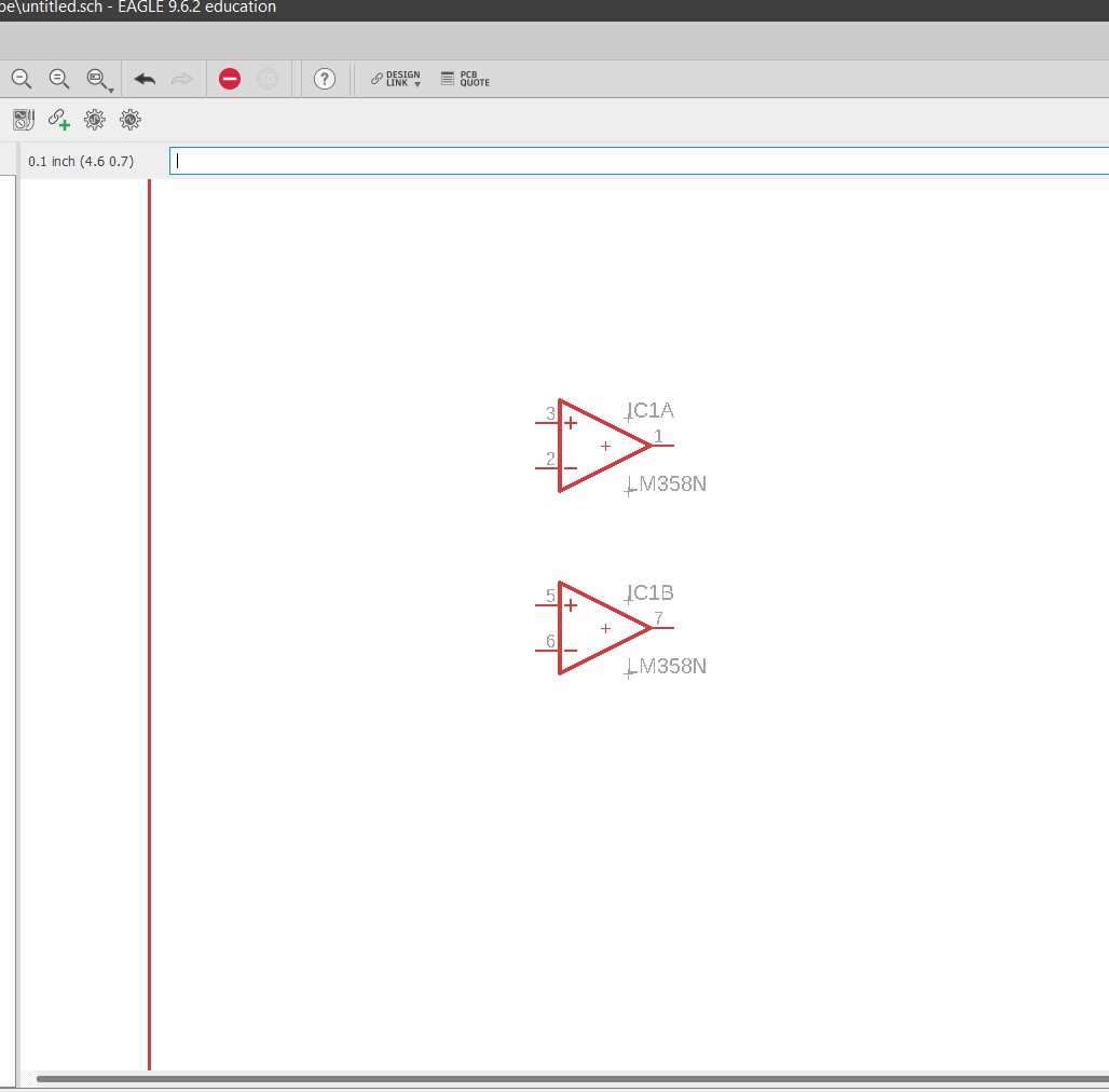
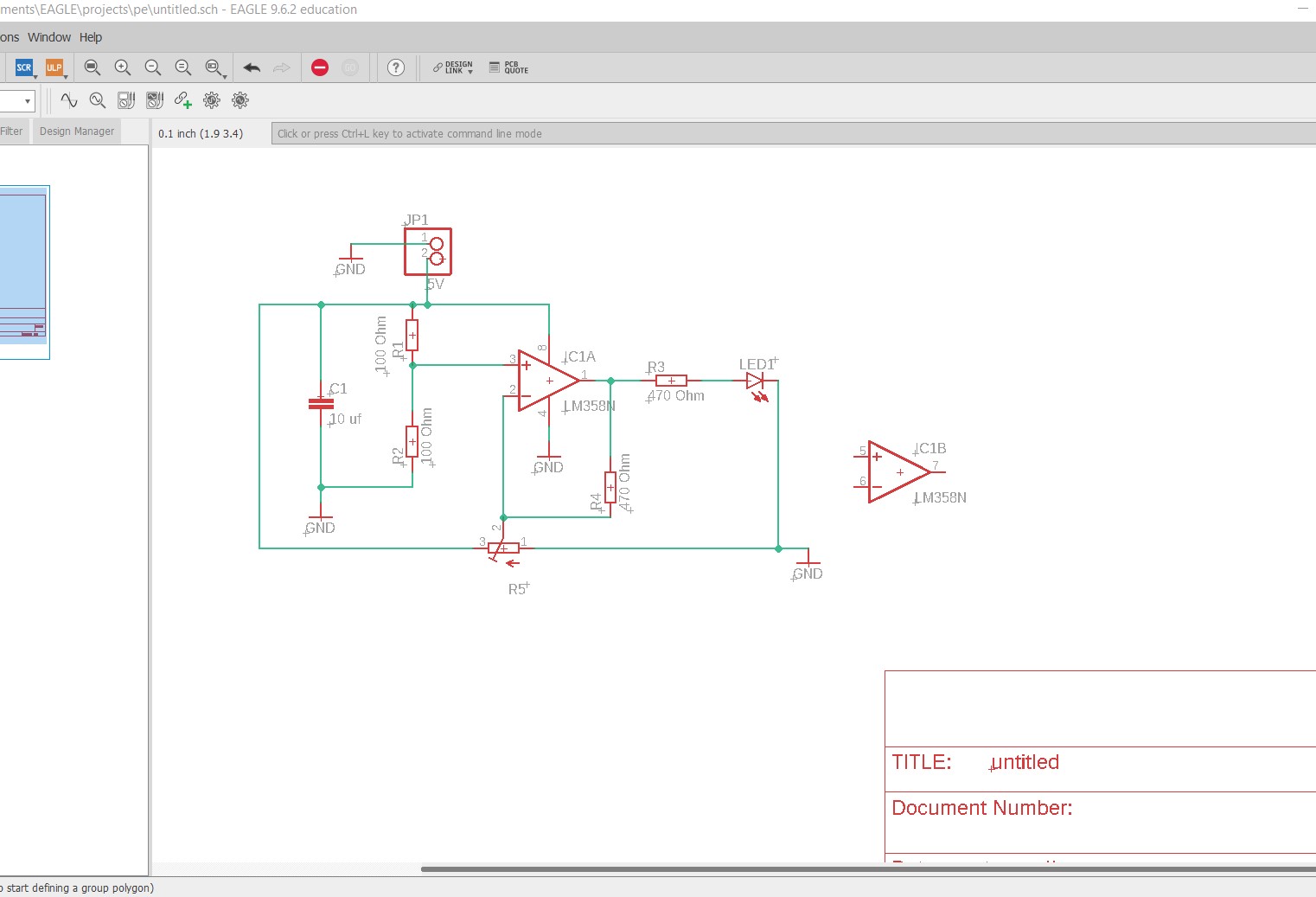
12. Type '*LM358*' into the search box and press 'Enter.' note that using the asters symbol * will show all parts with 'LM358' in their data. Expand and select the device's through-hole (THT) version, 'LM358N,' and click 'OK.' Click anywhere in the blank area to create the op-amp device. click again to get two devices named 'IC1A' and 'IC1B.'
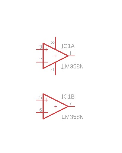
please be aware that the LM358 schematic symbol is separated in two parts
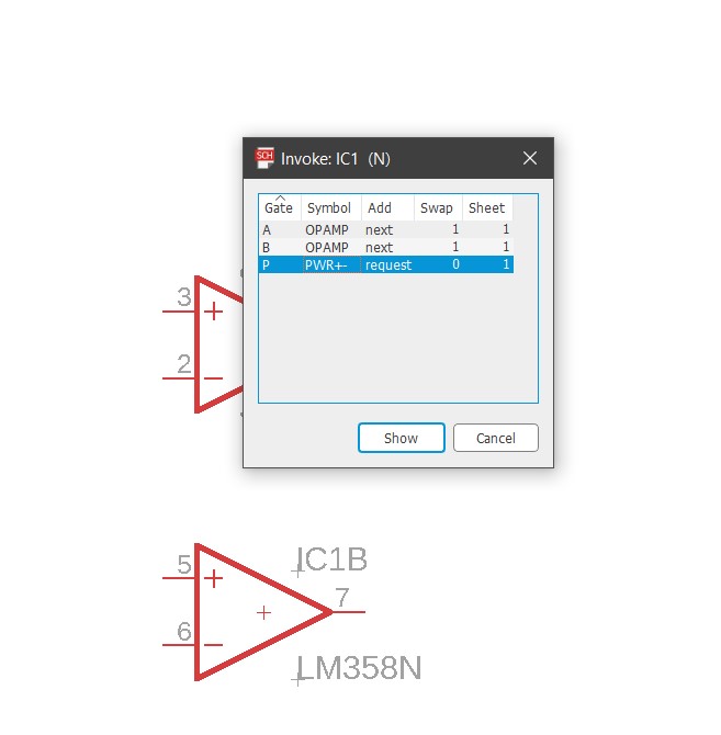
13. Press 'ESC' twice. Click the 'invoke' button on the left toolbar, then click on 'IC1A.' or right-click on 'IC1A. ' and select invoke In the menu, select Gate 'P' and press 'OK.' Place it onto the 'IC1A' device, making it look like the picture below.
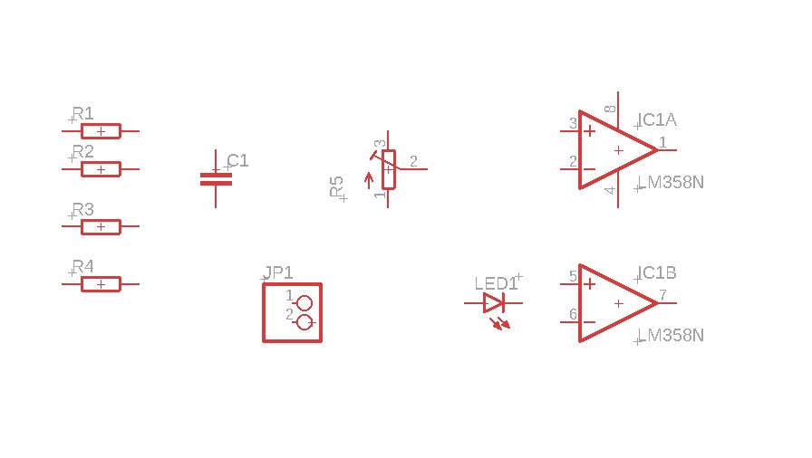
14. Now you should have a set of components like the picture below.
15. Go to 'File' and choose 'Save' to save your progress.
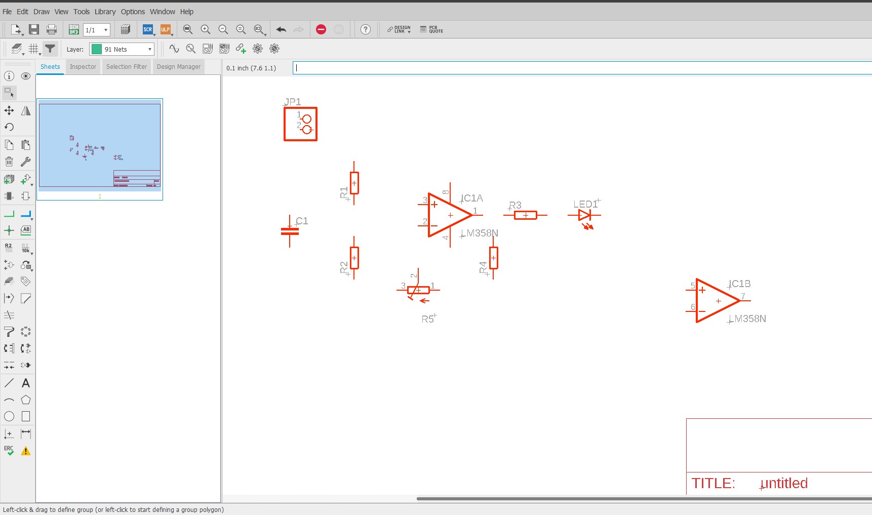
16. Use the 'move' tool to arrange the components, referring to the circuit diagram above. You can also use the 'rotate' tool to adjust component orientations. For renaming components, use the 'name' tool.
17. Click on the 'value' tool icon and then click on all resistors and capacitors to set their values.
18. Following the circuit diagram, Click on the 'net' tool to draw wires between relevant terminals. Click to terminate each wire.
19. Ensure all nets are correctly connected by using the 'junction' tool for interconnections.
20. From the 'supply1' library, add a ground pin (GND). If prompted for a net name, choose 'GND.' Connect different ground nets if necessary.
21. Also give the important nets name like 5V. Be aware that nets with the same name will be automatically connected even if you don't connect them like the GND in the picture below.
22. Your schematic should now be complete. Run an electrical rules check (ERC) to verify no mistakes. Click on the ’ERC’ button and make sure there are no errors and warnings you are not expecting.
Board
1. Save your schematic again and then choose File → Switch to board.
2. When asked if you would like to create the ’.brd’ file, click ’Yes’.
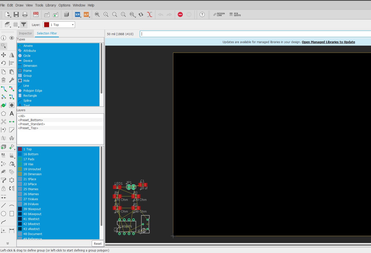
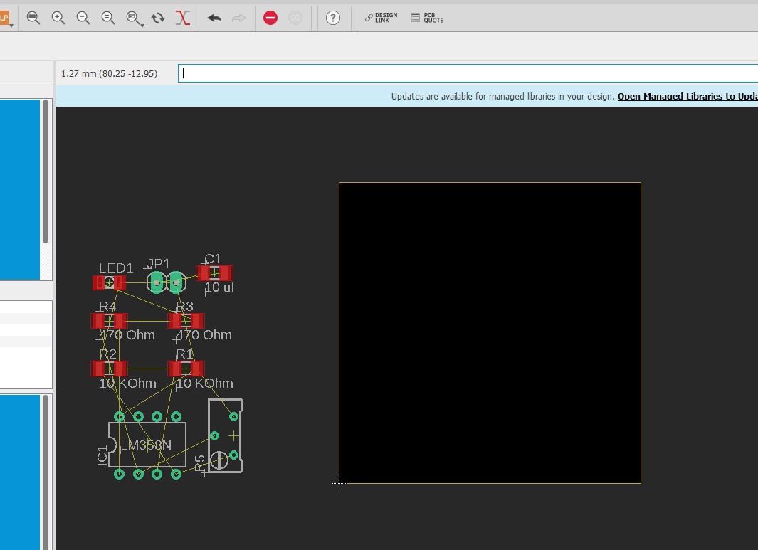
3. You will see a blank (black) board with all components in the lower left corner. The parts look different from the schematic because these are the actual footprints. It is the physical representation of a device and includes information about dimensions, holes, and copper areas that are needed to solder the device.
4. The first step is to set the grid to millimeters. To do that type ’grid mm;’ into the command line.
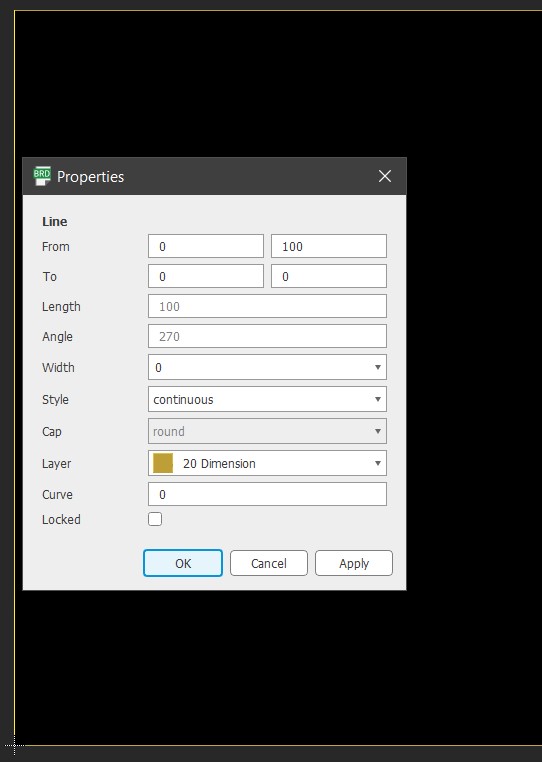
5. The next step is reducing the board size to 40 by 40 mm. Right-click on an edge, choose ’properties’ and then set the values appropriately. When you are done the board should be a square.
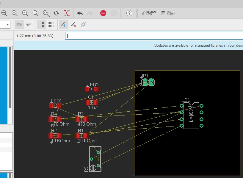
6. Use ’move’ and ’rotate’ to place all components inside the square area. Start with the IC and the connector. The connector should be placed close to the border of the board.
7. Place connected components near each other to minimize path length and path crossings. The yellow lines mark the connections you will have to route later.
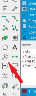
8. Click ’ ratsnest’ to force EAGLE to redraw the yellow lines.
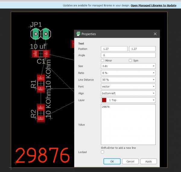
9. Use the ’Text’ tool to add your matriculation number to the board to be able to identify it in the upcoming labs. Click right on it and select ’properties’. Change size to 3.81 and select ’vector’ as font.
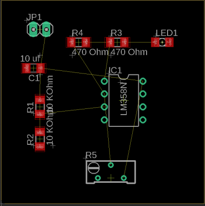
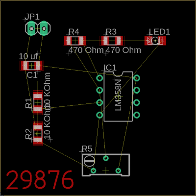
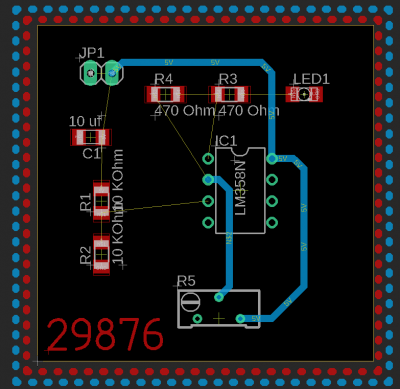
10. After the last step the board may look like the picture below.
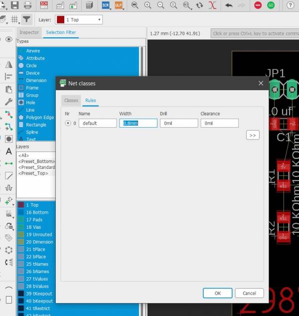
11. To set the default track size Go to Edit → net classes and change the width of the default net class to 0.8mm.
12. The next step is routing. There are two different approaches to this problem. Manual routing is described here.
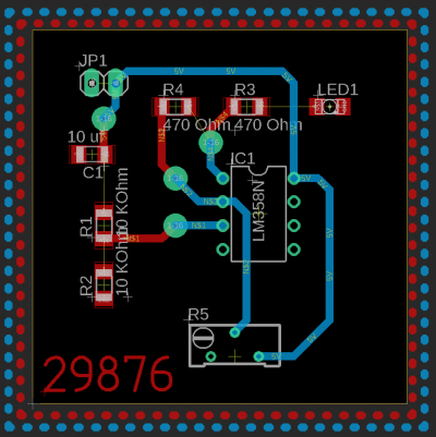
• Use the ’Route’ tool to make the actual connections. Pay close attention to the color of the route. Blue routes are on the bottom side of the board (layer 16), and red are on the top (layer 1).
• Since we want all our components to be on the top, the soldering for THT components will be on the bottom (layer 16) therefore all the connections for THT components should be on the bottom layer, and for SMD components on the top layer, you can use the ’Via’ tool to make a connection between top and bottom layer traces. The vias shall be round and have a diameter of 2.5 mm and a drill of 0.5 mm.
• Traces shall have a width of at least 0.8 mm. If yours is smaller you can use the ’change’ tool to set a bigger width.
• If a connection is made the yellow line should disappear. If it persists you have to look for the error.
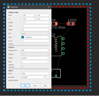
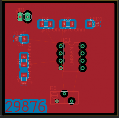
for a better and easier connection let’s define a ground plane on the bottom layer and top layer. use the ’polygon’ tool to make a rectangle around the dimension of your board.
13. Start by making GND polygons and don't forget to name it GND
14. start routing the connections
15. don't forget to add via to connect the top GND to the bottom GND with GND as the signal name

