Sidebar
Table of Contents
KiCAD Tutorial
KiCad is a free and open-source electronics design automation (EDA) suite. It features schematic capture, integrated circuit simulation, printed circuit board (PCB) layout, 3D rendering, and plotting/data export to numerous formats. KiCad also includes a high-quality component library featuring thousands of symbols, footprints, and 3D models. KiCad has minimal system requirements and runs on Linux, Windows, and macOS.
Where to download: https://www.kicad.org/download/
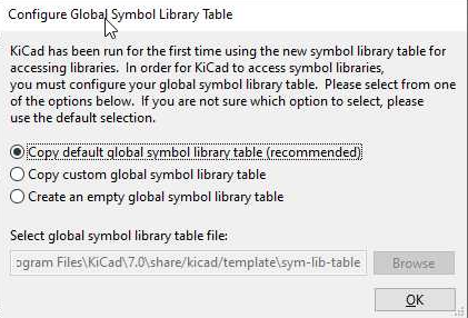
After downloading please use the recommended settings when prompted.
Introduction
The task is to design a PCB for Voltage Divider Circuit with LM358 Op-Amp, Potentiometer, and LED Output
Description:
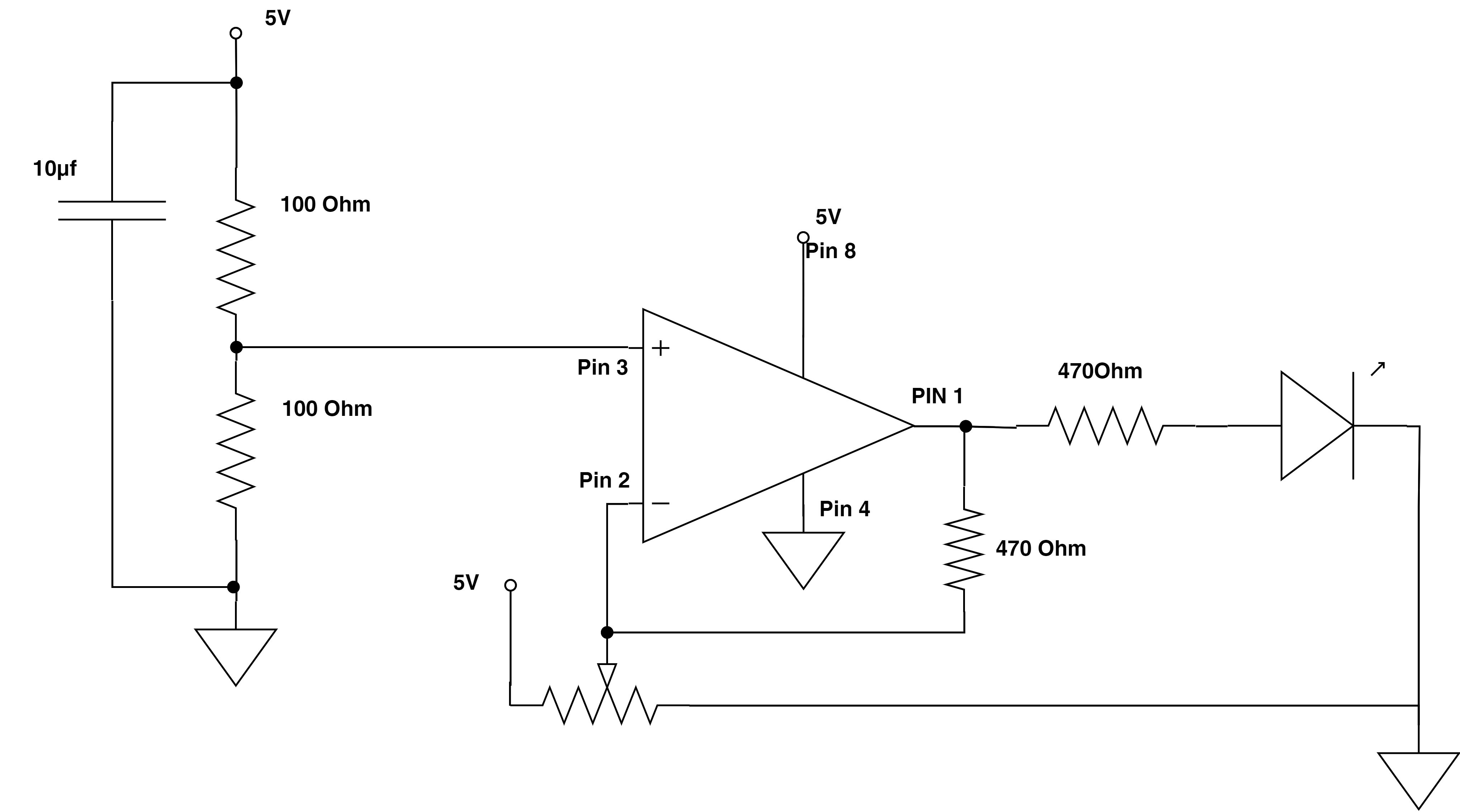
This circuit is designed to create a voltage divider using an LM358 operational amplifier (op-amp) with the output connected to an LED for visual output indication. The voltage to be divided is applied to the non-inverting input of the op-amp through a voltage divider, while a potentiometer is connected to the inverting input, allowing for voltage control.
Components:
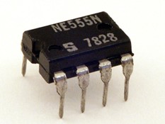
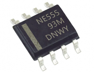
Remember the difference between through-hole technology (THT) and surface-mount device (SMD) components to choose the appropriate one based on the type of component you have
List of Components:
• LM358, Operational amplifier, Through hole, Two Op-Amps in one device
• Resistor, 2x10k, 2×470, SMD Package 1206, 4 pcs
• Capacitor, 10µF, SMD Package 1206, 1 pcs
• Pin Header, 1×2, THT, pitch 2.54mm
• potentiometer, THT, 10kOhm
• LED, SMD 1206, Green
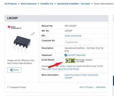
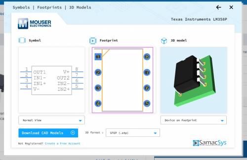
Every component has an ECAD model which includes a Circuit symbol for the schematic, a Footprint for the board layout, and a 3D Model https://www.mouser.de/ProductDetail/Texas-Instruments/LM358P?qs=X1HXWTtiZ0QtOTT8%252BVnsyw%3D%3D
Schematic Editor
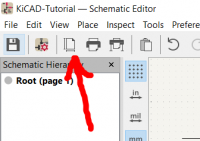
To open a new project go to File/New Project or press Ctrl + N. Name your project (e.g. KiCAD-Tutorial) and open the Schematic Editor.
Start off by editing the “Page Settings” (double-click) and filling out the title block. The intention is that you or someone else looking at the design at a later date will be provided some basic information at a glance.
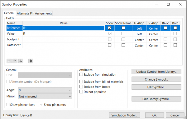
Adding Symbols, Power Symbols, Wires, Labels and more is quick and easy either using the right side taskbar or pressing A , P , W , L respectively. Start with a resistor. Press “A” on your keyboard and search for “R”, you will find the first result being a generic resistor symbol. Double-click it to choose as symbol you wanna place in your schematic. Now by moving your mouse the symbol moves with it, if you want to rotate the symbol simply press R and when you're happy with the location left-click once to paste it onto your schematic. If you are unhappy with your symbol choice simply press Esc once to remove the symbol or Esc twice to exit the add symbol function. Now you can do this for all symbols and edit the properties one by one later on. But when you know you're using the same footprint for more than one you can go ahead and double-click on the resistor you just pasted to open the symbol properties.
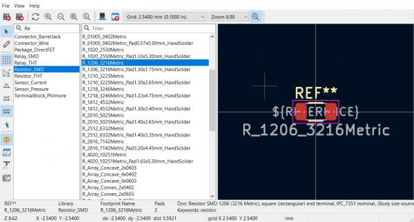
Now, click on footprint, this is where we assign a footprint to our symbol. Search for Resistor and choose Resistor_SMD library. There you will find all available footprints please choose sizes 1206 (or bigger) as it is otherwise quite hard to do hand assembly. Double-click the wanted footprint.
Now you're ready to select the resistor symbol by clicking on it once, pressing Ctrl + D to duplicate it as many times as you need. To undo the last action press Ctrl + Z or if you want to delete a specific symbol select it by clicking it once and to delete use the delete key.
Now repeating the same process we will add the remaining components
Capacitor:
- Press (A) and search for “C” and place the unpolarised capacitor symbol on your schematic
- Double Click on the symbol to enter the symbol properties
- Edit value, you can write 10uF
- Now click footprint and search for Capacitor_SMD in that library you will find C_1206_3216Metric
LED:
- Press (A) and search for “LED” and place the symbol on your schematic
- Double Click on the symbol to enter the symbol properties
- Edit value, you can leave it as LED
- Now click footprint and search for LED_SMD in that library you will find LED_1206_3216Metric
Potentiometer:
- Press (A) and search for “R-Potentiometer” and place the symbol on your schematic
- Double Click on the symbol to enter the symbol properties
- Edit value, you can write 10k
- Now click footprint and search for Potentiometer_THT in that library you will find Potentiometer_Bourns_3296W_Vertical
Connector:
- Press (A) and search for “Generic Connector” choose the Conn_01x02 and place the symbol on your schematic(Make sure its the generic one with the box around the pins not the “Connector” otherwise it can be difficult to see)
- Double Click on the symbol to enter the symbol properties
- Edit value, you can leave it as is
- Now click footprint and search for Connector_PinHeader_2.54mm in that library you will find PinHeader_1x02_P2.54mm_Vertical
LM358:
- Press (A) and search for “LM358” and place the symbol on your schematic
- Double Click on the symbol to enter the symbol properties
- Edit value, you can leave it as is, otherwise for another IC it would be preferable to write exact part name
- Now click footprint and search for Package_DIP in that library you will find DIP-8_W7.62mm
Now we have all our components but we need to add also power symbols. We can find a “power” library when using the already learned method with pressing (A). But there is a much easier solution. Just press (P) or alternatively the Add power smybol on the right side task bar. Press (P) on your keyboard and add symbols for +5V and GND.
Wire: Now you have everything only thing left to do is connect the symbols and add net labels. Either place your mouse cursor to one unconnected pin of any symbol it will by default offer to place a wire by showing you a green line and pus smybol if you wish to place a wire left click it and drag your mouse in the wanted direction. Double-click if you want to stop in clear space or left-click once to place a wired on another unconnected pin.
Important: Take care that parts often come in standard sizes and packages. For the potentiometer, we could have as well used just a 1×03 pin-header with 2.54mm spacing. So it is possible to reuse other footprints if making a symbol and footprint is undesirable.
The LM358B and LM2904B amplifiers are available in micro-sized packaging, such as the SOT23-8, as well as industry-standard packages including SOIC, TSSOP, and VSSOP. When choosing a footprint for the LM358 we don't look for LM358 but for the package we want to use. In our case it is the DIP-8 which we have in the lab and it stands for dual inline package with 8 pins.
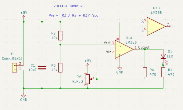
After adding all the components and making the connections you should have something like this:
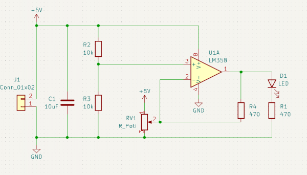 Fig. 5: Schematic
It is a good idea to put X or no connect marks on the pins you don't want to use (press Q) and place on the unused pins. Press (L) to add a net label, for example, Vin, Vref, Output, and led-res. After pressing (L) write the net label and press “Ok” then drag over and make sure to place the dot on the wire. After placing the labels we can double-click them to edit the size, name, orientation, etc. You can make the net label between the LED and resistor small because it's not very important to be seen but it will be very useful later when we come to the PCB layout. Additionally, it is very helpful to add text explaining some design choices or relevant calculations.
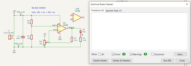
Before going to the PCB Editor make sure to do the Electrical Rules Check or ERC located on the top right. If you check now the Electrical Rules Check will complain about power pins not being driven by any power pins. This can be solved by adding another power symbol. Press (P) and search for PWR_FLAG and connect it to your GND and +5V. PWR_FLAG tells KiCad that the net that it is connected to has a power supply on it or in other words it is driven from somewhere.
General Recommendations
- Positive power rails( i.e. Vcc,+5V) point upwards, negative power rails and GND downward
- Part Symbols should never touch other part symbols
- Wires should cross part symbols
- Text should never touch any wires/symbols, other text
- Decoupling capacitors should be next to the parts they are supposed to decouple, not float randomly somewhere in the schematic
PCB Editor
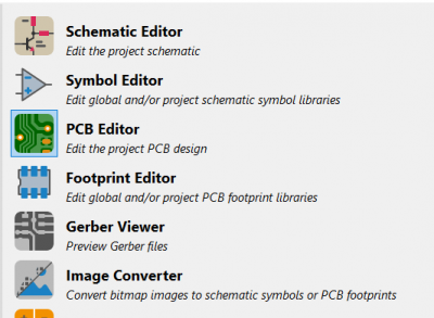
Now that we have our schematic and ERC is happy we can open the PCB Editor by either from the schematic clicking the second last button on the top taskbar or the third button from the project files window like so.
Schematic Editor window:

After doing so you will be surprised to see there is nothing but the frame in your PCB Editor.
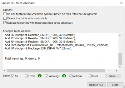
Continue by pressing (F8) on your keyboard or using the button on the top taskbar:
After pressing you should see no errors and no warnings.
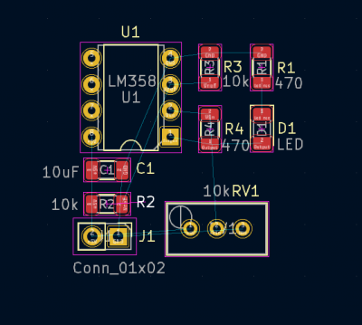
Press “Update PCB” and your components will appear in the top left corner. Now press “Close” and you will see all of your components are already selected and you can move your mouse to the middle of the frame a press once to drop and pres Esc to unselect them.
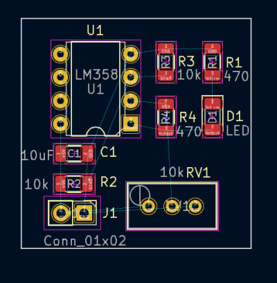
On the top taskbar select your grid. You can use 0.05 mm (0.002 in). Rearrange your components logically. You can do that by selecting them individually by left-clicking them and holding your left-click to drag them and (R) to rotate. Alternatively, after selecting a component you can press (M) on your keyboard and use the arrows for more precise positioning. After doing so you should come up with something like this:
Now change the grid to something big like 5.000 mm and click on the right side on the Edge.Cuts layer. And draw a rectangle with dimensions of 25 mm x 25mm. It will be easy to do so because of the 5mm grid. Alternativley you can always press Ctrl + Shift + M to measure with the ruler.
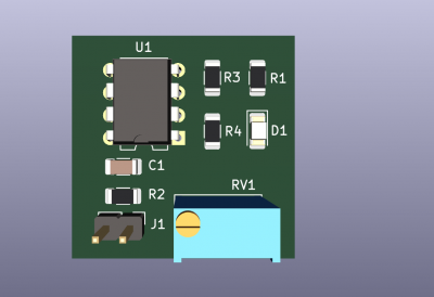
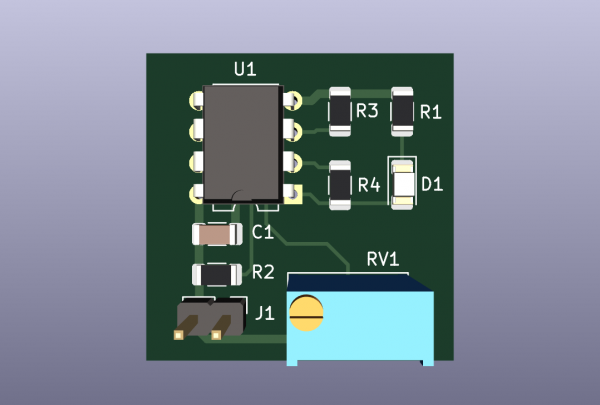
Press Alt + 3 on your keyboard to open the 3D view to check for mechanical constrains.
We see everything is okay we can proceed and whenever in doubt recheck the 3D model for a better intuitive oversight. While still in the sam grid press Ctrl + Shift + Z or the icon on the right taskbar “Added filled zone”.
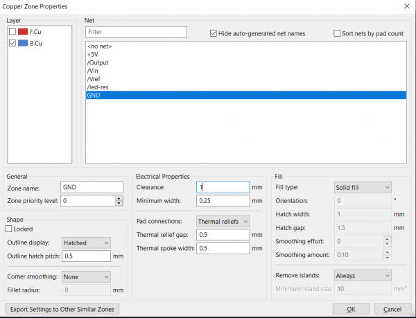
Select the B.Cu or bottom layer, select the GND net, you can name your zone GND, and leave the other settings the same but change the clearance to 1 mm like so.
Press B to fill the filled zone and Ctrl + B to unfill. Or alternatively, use the icons on the left taskbar to edit visibility.
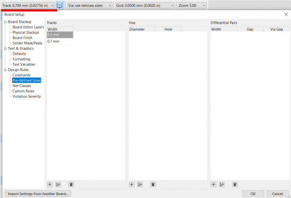
On to top left click “Track” and then Edit pre defined sizes. Add 0.3mm and 0.7mm and press okay.
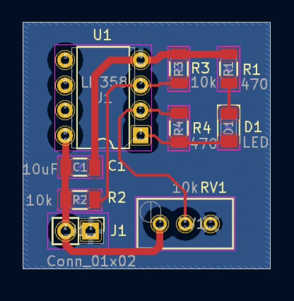
Now on the right size click the F.Cu for the front copper layer and click (X) to place tracks. Use thicker tracks for power and smaller ones for signals.
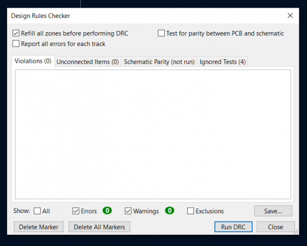
Finally, use the DRC (design rules checker) on the top right and Alt+3 for the 3D model to check if everything is in order.
Important note: Manufacturing capabilities can be found on the manufacturers websites, that includes tracks sizes clearances and so on. In the university we can produce only significantly larger track sizes with with 0.8 / 0.7 mm minimum as well as to keep in mind that THT components pads are not connected internally.

