User Tools
Sidebar
Table of Contents
This is an old revision of the document!
Applying solder mask to PCBs
Prerequisites
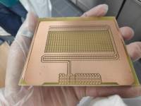
This instruction is about how to apply solder mask to PCBs. It is assumes you already have traces on a PCB (regardless of etched or milled) but no holes yet, like figure 1. You also need artwork (black printout to transparent foil) containing only pads (EAGLE layer 17) and vias (layer 18). Make sure it is really dark. We also suggest filling out the holes (you can use a black marker, e.g. this one or that one). The room you are working in has to been protected from of UV lights, e.g. use 05 EG 027. It has special lamps and no windows (avoiding sunlight).
Resources
Set up lab (figure ##). Other resorces are mentioned in the text.
Procedure
- Put on gloves to avoid fingerprints.
- Clean your PCB (using alcohol based solutions, e.g. ethanol).
- Take out the solder mask laminate. Cut two pieces slightly bigger than your PCB and pack the laminate back up again.
- Peel off the protective layer from the dim side (not the shiny side) of both pieces. Hint: apply tape to help removing the foil.
- Apply the laminate carefully to the PCB (figure ##). Avoid air bubbles at all cost because otherwise the solder mask will later break at these points after curing. Hint: use a credit card to evenly distribute pressure. Alternatively use the cold laminator for prepressing. If it's not going well, remove the laminate and try again with a new piece. You can use the development solution to strip of the laminate completely.
- Heat up the laminator and wait for it.
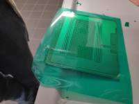
- Laminate. Multiple times if necessary. The result may look like figure 4
- Chill PCB with cold water. (Necessity of chilling is questionable.)
- Align the artwork to your PCB and tape it.
- Expose it with UV light for 60 seconds (setting 1|0|0). You should wait for the vacuum to build before you start the exposing.
- Take out the PCB and wait for 5 minutes. (Necessity of waiting is questionable.)
- Remove the second protective foil (on the shiny sides).
- Cut of excessive laminate.
- Put on your other personal protective equipment (goggles, lab coats).
- Set up development solution, leftovers from etching process can be used. Normal developer would be 5g sodium hydroxide in 250 ml (purified) water. Lower concentrations lead to longer developing times, which can be beneficial for better handling.
- Develop for 60 seconds (assuming new strong solution). Look out for color changes. The pads/vias should become turquoise.
- Remove solder mask on pads/vias mechanically with toothbrush.
- Rinse PCB with (purified) water and wait for 5 minutes. (Necessity of waiting is questionable.)
- Dry the PCB for example by feeding it again multiple times through the hot laminator but covered with baking paper.
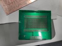
- Complete the curing of the solder mask by exposing it further for 20-30 minutes or leaving the PCB at a place with sunlight for a day (figure 5).
- Go on like in a usual PCB manufacturing process (drill holes, punch via, solder).
 Fig. 1: Etched PCB
 Fig. ##: Lab setup
 Fig. ##: Prepare for lamination
 Fig. 4: Laminated
 Fig. 5: Finished
